
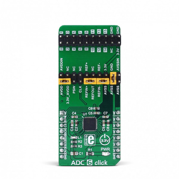
ADC 6 click


Prices incl. GST
Out of Stock.
- Product Code: MIKROE-2932
- MPN: MIKROE-2932
A precise ADC module with flexible signal routing
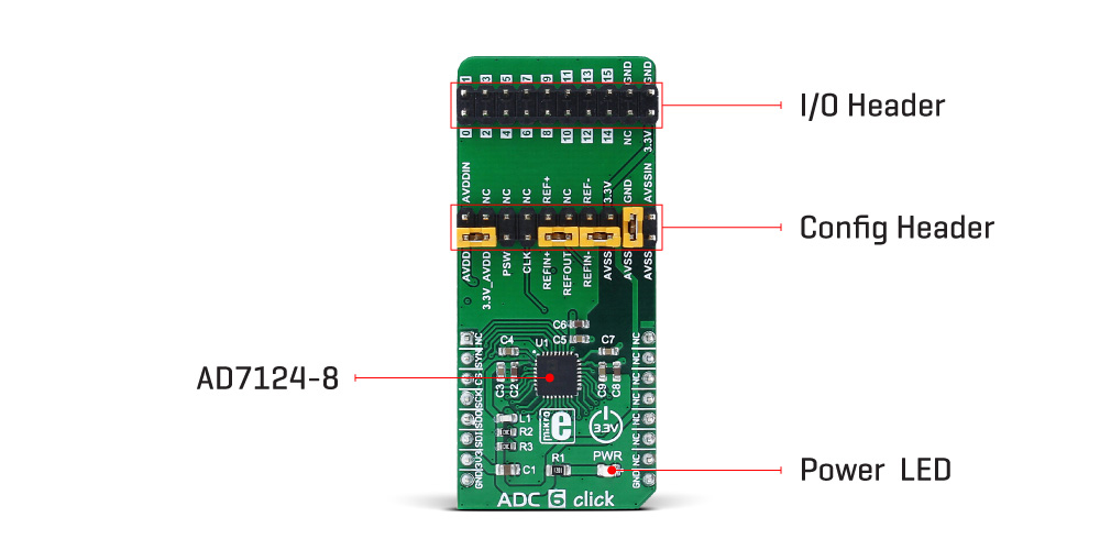
ADC 6 click is an advanced 24bit multichannel analog to digital converter (ADC), with 8 fully differential or 15 single-ended/pseudo differential sampling inputs, and very flexible routing capabilities. The click board™ has two 2x10 pin headers, used both to configure the device and connect the input channels. This allows for unrestrained configuration of the device, so it can use both bipolar and unipolar input sources, with selectable reference voltages, external clock, auxiliary power switch, and more.
Packed with many features - including a reliable and extensive diagnostic functions - among others, ADC 6 click can be used for an analog to digital conversion in various applications, such as precise temperature or pressure measurement, manufacturing process control, precise instrumentation in general, and for similar applications that can benefit from reliable AD conversion with high accuracy.
How does it work?
The main active component of the ADC 6 click is the AD7124-8, an 8 channel, low noise, low power, 24bit sigma-delta ADC with reference and programmable gain array, from Analog Devices. This IC offers several different power modes and input connection configurations, giving a lot of flexibility to work with. The device can have 8 differential or 15 pseudo differential analog inputs, as well as any combination between them. All the input channels can be configured to be either buffered or unbuffered, depending on the input connection impedance characteristics. The maximum output data rate varies from 2400 SPS up to 19,200 SPS (samples per second), in respect to the selected power mode. An ultra-low noise operation results with having 22 noise free bits in all available power modes.
The signal routing in the AD7124-8 ADC is done via the internal multiplexer section, which is used to reduce the number of IC pins, yet allowing all of the functions to be used on the existing pins. On a top of these pins, there are four more GPIO pins that can be used for various tasks, including control of the multiplexer unit. Since the multiplexer is integrated into the chip, the conversion process stays synchronized with the changes made to the pin configuration.
The input signal is further managed by so-called setups. There are eight such setups available on the AD7124-8 ADC module. A single setup consists of four different registers: configuration register, filter register, gain register and offset register. Those registers are used to configure the corresponding set of functions for the connected channel(s). The channel register itself is used to configure the basic settings for the corresponding ADC channel, and among other options, which of the eight available setups to connect with that channel. This mechanism allows easy configuration of multiple channels, especially when the same settings need to be applied to more than one channel, greatly reducing the software complexity, since the setups can be reused.
An internal bias voltage generator can be routed to the output pins. It is used to bias the negative terminal of the selected input channel. This function is useful in thermocouple applications, as the voltage generated by the thermocouple must be biased around some DC voltage when the ADC operates from a single power supply.
The AD7124-8 ADC module is clocked by either an internal clock source, which works at 614.4 kHz. The CLK pin can be used either to output the clock signal available on the ADC or to use the external clock input. This allows synchronizing of several devices by using the same clock frequency. The internal clock speed is divided, depending on the selected operating mode. Selecting low power operating modes will have an impact on the samples per second which this device can perform.
ADC 6 click uses the SPI interface for communication with the host MCU. The SPI bus pins are routed to the mikroBUS™ SPI pins (MISO, MOSI, SCK, and CS), allowing an easy integration with the development system. The device uses the SPI mode 3, which means that the clock signal (SCK) is idle HIGH, and the rising edge of SCLK is the sample edge. The data is clocked out on the falling edge and clocked in on the rising edge of the clock signal pulse.
The Data Out pin of the ADC module (DOUT/#RDY) is routed to the mikroBUS™ MISO pin, and besides for the data output, is also used to signal the presence of the valid data in the ADC output shift register. When there is a valid reading stored to this register, the #RDY signal will be pulled to a LOW state, indicating the ready status of the data output register. It can be used to trigger an interrupt on the host MCU.
The #SYNC pin of the ADC module is used to synchronize reading when more than one device is used. While pulled to a LOW state, the internal ADC sections are reset and held in the reset state. This pin is pulled to a HIGH logic level via the onboard resistor. This pin is routed to the mikroBUS™ RST pin. There is a number of pins routed to the 2x10 standard pitch of 2.54mm (100mils) header. This allows even easier routing with jumpers or jumper wires, as the header can be used to further configure the ADC in a way that is impossible by software, i.e. connecting an external clock source or reference voltages. The complete layout of this header can be seen on the schematics of the ADC 6 click. The second 2x10 header is used to connect the input signals. The AD7124-8 ADC module allows several kinds of signals to be routed to these pins via the multiplexing section, allowing diagnostic functions to be interleaved with the conversion of the analog signals.
To ensure an accurate input signal conversion, the device features a thermal sensor, which can be used to compensate for the ambient temperature. This thermal sensor is embedded into the ADC module and it is used to measure the die temperature. It can be selected as a conversion source so that the die temperature can be calculated according to the formula that can be found in the AD7124-8 datasheet.
The provided library functions allow easy configuration of the ADC 6 click, as well as reading the conversion data. The included demo application can be used as a reference for future designs.
Specifications
| Type | ADC |
| On-board modules | AD7124-8 ADC module |
| Key Features | 24bit multichannel analog to digital converter, 8 fully differential or 15 single ended/pseudo differential sampling inputs |
| Interface | GPIO,SPI |
| Input Voltage | 3.3V |
| Click board size | L (57.15 x 25.4 mm) |
Pinout diagram
This table shows how the pinout on ADC 6 click corresponds to the pinout on the mikroBUS™ socket (the latter shown in the two middle columns).
| Notes | Pin | Pin | Notes | ||||
|---|---|---|---|---|---|---|---|
| NC | 1 | AN | PWM | 16 | NC | ||
| Synchronization | SYN | 2 | RST | INT | 15 | NC | |
| SPI Chip Select | CS | 3 | CS | RX | 14 | NC | |
| SPI Clock | SCK | 4 | SCK | TX | 13 | NC | |
| SPI Data Out/RDY | SDO | 5 | MISO | SCL | 12 | NC | |
| SPI Data In | SDI | 6 | MOSI | SDA | 11 | NC | |
| Power supply | +3.3V | 7 | +3.3V | 5V | 10 | NC | |
| Ground | GND | 8 | GND | GND | 9 | GND | Ground |
ADC 6 click electrical specifications
| Description | Min | Typ | Max | Unit |
|---|---|---|---|---|
| Output Data Rate (power mode dependent) | 1.17 | 19,200 | SPS | |
| Absolute Input/Reference Voltage (unbuffered) | AVSS−0.05 | AVDD+0.05 | V | |
| Absolute Input/Reference Voltage (buffered) | AVSS+0.1 | AVDD-0.1 | V | |
| External Reference Voltage Range(1) | 1 | 2.5 | AVDD | V |
| Internal Reference Voltage Range(1) | 2.5-0.2% | 2.5 | 2.5+0.2% | V |
Note: (1) States the reference/input voltage ranges, not the actual reference/input voltage values. These voltages can be of both bipolar and unipolar type: e.g. 1V means -0.5V to +0.5V, the same as 0V to +1V
Onboard settings and indicators
| Label | Name | Default | Description |
|---|---|---|---|
| LD1 | PWR | - | Power LED indicator |
| CN1 | - | - | I/O Header |
| CN2 | - | On schematic | Configuration Header |
Note: The default configuration jumpers position can be seen in the provided schematic of the ADC 6 click board. The pin functions are clearly marked on the print layer of the PCB
Software support
We provide a library for ADC 6 click on our Libstock page, as well as a demo application (example), developed using MikroElektronika compilers and mikroSDK. The provided click library is mikroSDK standard compliant. The demo application can run on all the main MikroElektronika development boards.
Library Description
Initializes and defines SPI bus driver and driver functions which offer a choice to convert an analog input voltage to a 24-bit digital output value. Functions also offer a choice to choose which channels we want to use for positive and negative analog input by writing in configurations registers. Functions can read converted data in two modes, single read, where we must be sure that converting is done, or continuous read mode, where we only continuously read converted data without writing anything on SPI, not even a data register address. Library also defines commands which help us to configure registers. Check the documentation for more details.
Key functions :
void adc6_writeReg( const uint8_t register_address, const uint32_t transfer_data ) - Function writes data to the determined register.
uint32_t adc6_readReg( const uint8_t register_address ) - Function reads data from the determined register.
uint32_t adc6_continuousReadData( void ) - Function continuously reads data from Data register without writing anything on SPI.
uint32_t adc6_getADCData( const uint8_t mode ) - Function gets data from Data register in two possible modes. In single read mode first checks ready bit, and when the conversion is done (data is ready) reads data from the register. In continuous read mode only reads data without writing anything on SPI bus.
Examples Description
The application is composed of three sections :
- System Initialization - Initializes peripherals and pins.
- Application Initialization - Initializes SPI bus driver and sets configuration which enables channel 0, puts AIN0 on positive analog input and AIN1 on negative analog input, enables internal reference voltage (approximately 2.65V, AVDD = 3.3V), and also enables bipolar operation mode and puts the device on full power mode. When the ADC is configured for unipolar operation, the output code is natural (straight) binary with a zero differential input voltage resulting in a code of 0x00000000, a midscale voltage resulting in a code of 0x00800000, and a full-scale input voltage resulting in a code of 0x00FFFFFF. When the ADC is configured for bipolar operation, the output code is offset binary with a negative full-scale voltage resulting in a code of 0x00000000, a zero differential input voltage resulting in a code of 0x00800000, and a positive full-scale input voltage resulting in a code of 0x00FFFFFF.
- Application Task - (code snippet) - Gets 24-bit converted data in single read mode and logs data on USB UART. Repeats operation every 500 ms.
void applicationTask()
{
adc_value = adc6_getADCData( _ADC6_SINGLE_GET_DATA_MODE );
LongWordToStr( adc_value, text );
if ( tmp )
{
mikrobus_logWrite( "** The ADC value is: **", _LOG_LINE );
tmp = 0;
}
mikrobus_logWrite( text, _LOG_LINE );
Delay_ms( 500 );
}
The full application code, and ready to use projects can be found on our LibStock page.
Other mikroE Libraries used in the example:
- Conversions
- SPI
- UART
Additional notes and information
Depending on the development board you are using, you may need USB UART click, USB UART 2 click or RS232 click to connect to your PC, for development systems with no UART to USB interface available on the board. The terminal available in all MikroElektronika compilers, or any other terminal application of your choice, can be used to read the message.
mikroSDK
This click board is supported with mikroSDK - MikroElektronika Software Development Kit. To ensure proper operation of mikroSDK compliant click board demo applications, mikroSDK should be downloaded from the LibStock and installed for the compiler you are using.