
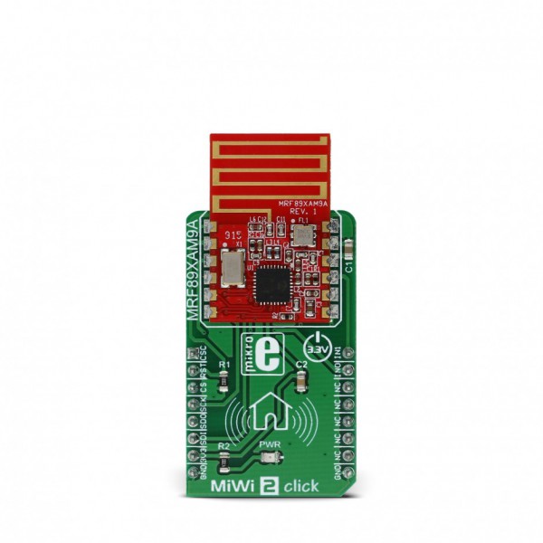
MiWi 2 click


Prices incl. GST
Out of Stock.
- Product Code: MIKROE-2925
- MPN: 2925
MiWi 2 click is a sub-gigahertz radio transceiver click board™, which offers a reliable FSK or OOK communication solution, with the maximum data rates of 200kbps and 40kbps, respectively. The radio transceiver module used on this click board™ has plenty of features that make it a perfect choice for compact designs: It has very good reception sensitivity, an onboard PCB antenna, high level of components integration, built in packet handling routines with automatic CRC generation, 64 bytes of transmit/receive FIFO buffer, built in Sync Word recognition, clock/data synchronisation and recovery and many more.
Armed with such a powerful, compact and fully configurable radio transceiver module, MiWi 2 click offers highly reliable radio communication over a short distance, which can be utilized in many applications. It can be used for developing home/industrial/building automation applications, data loggers, applications for remote keyless access, alarms, wireless remote control and a wide variety of similar short-range radio applications.
Note: This click board complies with the United States (FCC Part 15.247 and 15.249) regulatory standards. For European (ETSI EN 300-220) regulatory standards compliant click board, please visit the product page of the MiWi click.
HOW DOES IT WORK?
MiWi 2 click features the MRF89XAM9A, a compact low-power sub-gigahertz radio transceiver module from Microchip, that operates at a frequency range between 902MHz and 928MHz. This module has all the necessary components onboard, including a small trace PCB antenna and matching electronics, allowing compact design, while maintaining the flexibility. It supports OOK and FSK signal modulation with data rates limited to 200kbps and 40kbps respectively, in order to be compliant with the ETSI standards. The MRF89XAM9A module is based upon a base architecture of the generic MRF89XA module, with a few modifications, applied in order to make this module FCC and IC standards compliant.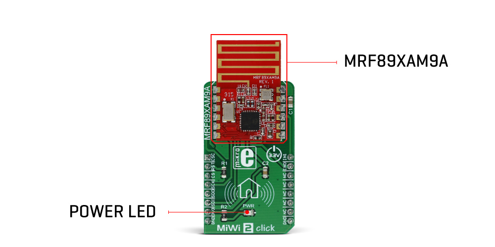
The module uses the SPI communication protocol. However, it uses two chips select lines, #CSCON - config block select and #CSDATA - data block select, used to access a different group of internal registers. These two lines are routed to the mikroBUS™ AN and CS pins, respectively. It should be noted that the device only supports SPI mode 0, 0 - which means that the serial clock signal (SCK) is idle LOW. Pulling the #CSCON line to a LOW logic level will enable communication with the configuration registers. Pulling the #CSDATA will enable host communication with the FIFO buffer. If both chip select lines are pulled to a LOW logic level, the #CSCON will have a priority over the #CSDATA.
The data processing section is used to interface the data from the MODEM (modulator/demodulator) section, with the host MCU access point sections (SPI and IRQ sections). The data processing section contains several control blocks that manage the data traffic. The data processing section supports 2 modes of operation of which are available on the MiWi 2 click:
- Buffered mode - the transmitting or received data is stored in the FIFO buffer and available via the SPI
- Packet mode - packets of certain structure are stored in the FIFO buffer, max 64 bytes
These modes affect the host MCU processing overhead. In the Buffered mode, the host MCU has to manage sending or receiving of the preamble, Sync Word, and the actual payload, relying on the IRQs to get the FIFO buffer status and manually managing the number of sent/received bytes.
The FIFO (First In First Out) register performs parallel operations and it is 8 bits wide. However, the RF demodulator section works only with serial data, sending and receiving the information bit by bit, with the programmed rate. To interface FIFO buffer with the demodulator section, a shift register has to be employed. The FIFO register serves as a buffer for both data transmission and reception.
Two interrupt request lines (IRQ0 and IRQ1) of the MRF89XAM9A module are routed to the mikroBUS™ pins INT and PWM, respectively. These pins can be configured to generate an interrupt request to the host MCU, depending on the selected events. There are many interrupt sources that can be selected to trigger an interrupt. Before using interrupts, they have to be unmasked and enabled. All the interrupt sources and flags are configured through the Interrupt Configuration registers.
RESET line from the module is routed to the mikroBUS™ RST pin and it is used to reset the device. After the reset, the device is unavailable for about 5ms. To reset the device, this pin has to be pulled to a HIGH logic level for at least 100 µs. It is pulled to a LOW logic level by the pull-down resistor.
The OOK and FSK modulation protocols are commonly used subgigahertz protocols and each has its own benefits. In OOK mode (Off On Keying), the carrier signal is amplitude modulated by switching between no carrier signal for the logical 0 and full carrier amplitude signal for the logical 1. The FSK (Frequency Shift Keying) modulation is basically frequency modulation with two different frequency values for the logical 0s and 1s. MiWi 2 click is able to modulate and demodulate signals by using both of these protocols.
The provided libraries contain functions for an easy and simplified configuration of MiWi 2 click. The included demo application can be used as a reference for future design and it demonstrates usage of the provided functions.
SPECIFICATIONS
| Type | Sub-1 GHz Transceievers,MiWi |
| Applications | It can be used for developing home/industrial/building automation applications, data loggers, applications for remote keyless access, alarms, wireless remote control and a wide variety of similar short-range radio applications. |
| On-board modules | MRF89XAM9A, a compact low-power sub-gigahertz radio transceiver module from Microchip |
| Key Features | It has very good reception sensitivity, an onboard PCB antenna, high level of components integration, built in packet handling routines with automatic CRC generation, 64 bytes of transmit/receive FIFO buffer, built in Sync Word recognition, etc. |
| Interface | GPIO,SPI |
| Compatibility | mikroBUS |
| Click board size | L (57.15 x 25.4 mm) |
| Input Voltage | 3.3V |
PINOUT DIAGRAM
This table shows how the pinout on MiWi 2 click corresponds to the pinout on the mikroBUS™ socket (the latter shown in the two middle columns).
| Notes | Pin | Pin | Notes | ||||
|---|---|---|---|---|---|---|---|
| Config Block CS | CSC | 1 | AN | PWM | 16 | IN1 | IRQ pin 1 |
| Reset | RST | 2 | RST | INT | 15 | IN0 | IRQ pin 0 |
| Data Block CS | CS | 3 | CS | RX | 14 | NC | |
| SPI Clock | SCK | 4 | SCK | TX | 13 | NC | |
| SPI Data Out | SDO | 5 | MISO | SCL | 12 | NC | |
| SPI Data In | SDI | 6 | MOSI | SDA | 11 | NC | |
| Power supply | +3.3V | 7 | 3.3V | 5V | 10 | NC | |
| Ground | GND | 8 | GND | GND | 9 | GND | Ground |
MIWI 2 CLICK SPECIFICATIONS
| Description | Min | Typ | Max | Unit |
|---|---|---|---|---|
| Frequency Range | 902 | 928 | MHz | |
| Bit Rate (FSK) | 2 | 200 | kbps | |
| Bit Rate (OOK) | 1.56 | 28 | kbps | |
| SPI Configure Clock Frequency | 6 | MHz | ||
| SPI Configure Data Frequency | 1 | MHz | ||
| FSK reception sensitivity at 25kbps | -105 | dBm | ||
| OOK reception sensitivity at 2 kbps | -111 | dBm | ||
| Typical output power | +10 | dBm |
ONBOARD SETTINGS AND INDICATORS
| Label | Name | Default | Description |
|---|---|---|---|
| LD1 | PWR | - | Power LED indicator |
SOFTWARE SUPPORT
We provide a library for MiWi 2 click on our Libstock page, as well as a demo application (example), developed using MikroElektronika compilers and mikroSDK. The provided click library is mikroSDK standard compliant. The demo application can run on all the main MikroElektronika development boards.
Library Description
Library carries generic functions which are enough to have complete control over MiWi 2 click.
Key functions
void miwi2_writeReg(uint8_t address, uint8_t value)- Writes data to the register
uint8_t miwi2_readReg(uint8_t address)- Reads data from the register
void miwi2_writeFIFO(uint8_t Data)- Writes data to the FIFO buffer
uint8_t miwi2_readFIFO()- Reads data from the FIFO buffer
Examples Description
Demo application is modified version of Microchip's application for MRF89XA devices. Application is in the form of a console app with simple UI which allows operations such as register_read or write but also TX and RX routines.
This function (code snippet) continuously transmits predefined packet with delay of 100 ms between each transaction.
void RadioApp_txPredefinedPacket()
{
uint8_t input;
uint8_t tmpPacket[ 6 ] = { 80, 65, 67, 75, 69, 84 };
ConsolePut_constString("Transmitting predefined packet at");
RadioApp_printMiniStatus(PR_TX_MODE);
ConsolePut_constString("Press (Ctrl+z) to exit");
ConsolePut_newLine();
while (1)
{
if (ConsoleGet_ready())
{
input = ConsoleGet();
ConsolePut(input);
if (input == 26)
return;
}
miwi2_sendPacket(&tmpPacket[0], 6);
_miwi2_rfMode = _MIWI2_RF_STANDBY;
Delay_ms( 100 );
}
}
The full application code, and ready to use projects can be found on our Libstock page.
Other MikroElektronika libraries used in the example:
- SPI
- UART
Additional notes and information
Depending on the development board you are using, you may need USB UART click, USB UART 2 click or RS232 click to connect to your PC, for development systems with no UART to USB interface available on the board. The terminal available in all MikroElektronika compilers, or any other terminal application of your choice, can be used to read the message.
MIKROSDK
This click board is supported with mikroSDK - MikroElektronika Software Development Kit. To ensure proper operation of mikroSDK compliant click board demo applications, mikroSDK should be downloaded from the LibStock and installed for the compiler you are using.
For more information about mikroSDK, visit the official page.