Prices incl. GST
Ready to ship today,
Delivery time appr. 1-3 workdays.
1 in stock
- Product Code: MIKROE-2963
- MPN: MIKROE-2963
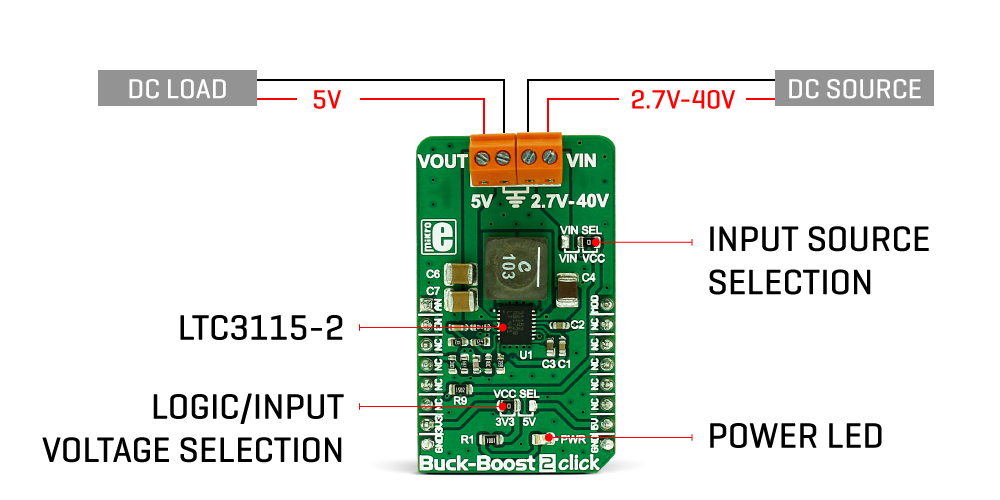
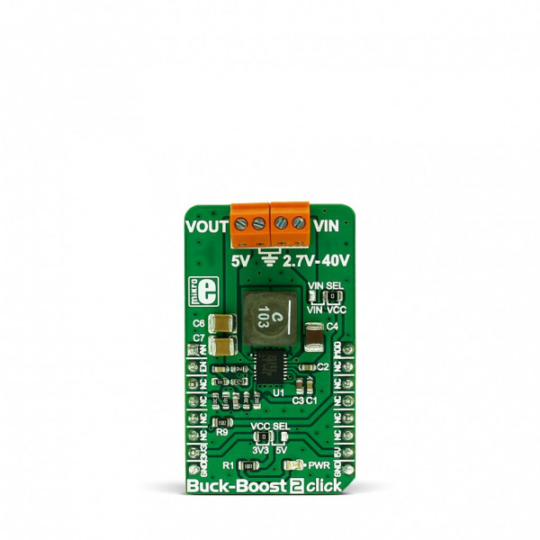
Buck-Boost 2 click is an advanced DC-DC step-down/step-up regulator (buck/boost), which is able to provide regulated 5V on its output, regardless of the input voltage. The input voltage can range from 2.7V up to 40V. The click board™ provides an ultra-low noise and ripple free regulated output, with transparent switching from a buck to boost mode - depending on the input voltage, which produces no discontinuities or switching artifacts, such as transients or subharmonic switching. Selectable switching mode allows optimal power consumption and high power efficiency, for both lighter and heavier loads.
Featuring a range of advanced regulation, protection and switching functions, this Click board™ can be used to provide a clean and regulated 5V output from a range of different unregulated sources, such as lead-acid battery cells, firewire connectors, or unregulated wall adapters, with enough current to drive most applications that require stabilized 5V power supply.
How does it work?
Buck-Boost 2 click is equipped with the LTC3115-2, a 40V, 2A synchronous buck-boost DC/DC converter from Linear Technology. This IC relies on the advanced four MOSFET switch topology, so it can sustain the regulation in both cases when the input voltage is lower and higher than the output voltage, set by the feedback network to 5V. A proprietary switching algorithm ensures transparent, continuous transition between operating modes. The LTC3115-2 features both forward and reverse current limiting section. The maximum current available on the output depends on the mode of operation: If the output voltage is greater than the input voltage, the device works in boost mode and the maximum current is about 0.6A. If the output voltage is less than the input voltage, the device works in buck mode and the maximum current available is about 1.4A. Also, the maximum output current is affected by the switching mode, selectable by the MODE pin, routed to the PWM pin of the mikroBUS™. There are two modes available: fixed frequency PWM mode and burst mode.

While working in PWM mode, the LTC3115-2 IC uses a fixed frequency, determined by the onboard resistor - in the case of the Buck-Boost 2 click, it is fixed at 750kHz. The PWM mode is used when a heavier load is connected to the output terminal. This mode is set when the PWM/SYNC pin is pulled to a HIGH logic level. This mode allows the maximum current on the output and results with the lowest amount of switching noise and output voltage ripple. This mode is used to provide the power for the connected devices, while they work in the active mode.
The burst mode is used for maintained efficiency when light output loads are used. The device will work in burst mode when the PWM/SYNC pin is pulled to a LOW logic level. While in burst mode, the variable frequency switching algorithm is used, resulting in a very low quiescent current, which allows lowered power consumption - e.g. when the external voltage input is taken from a battery. The error amplifier is powered down in this mode and the output current should not be greater than allowed, else the output voltage will lose regulation. This mode is perfectly suited to power up various devices while they work in standby mode.
When using the synchronization function of the PWM/SYNC pin, the device works in the fixed frequency PWM mode, but its frequency is regulated by the external clock source, by the means of the internal PLL section. This can be useful when special power supply noise requirements must be met. Since the internal PLL is able only to increase the internal clock frequency, the external clock signal should be above the frequency set by the onboard resistor (750kHz) taking the sufficient error margin into account.
The RUN pin of the LTC3115-2 IC is routed to the mikroBUS™ RST pin and it is used to activate the internal logic and switching circuitry. Setting this pin to a HIGH logic level (above 1.21V) will enable both the logic and the switching sections of the LTC3115-2 IC.
It is possible to measure and monitor the output voltage of the Buck-Boost 2, by utilizing the voltage divider, with its middle point routed to the AN pin of the mikroBUS™. By applying the calculation from the formula below, it is possible to determine the exact value of the output voltage. It can be used to monitor the output so that the appropriate action can be taken in the case when the voltage drops or loses regulation. The output voltage can be derived from the following formula:
VAN = (R10/(R10+R11)) x VOUT
Where R10 = 10K? and R11 = 6.8K?. For the output voltage of 5V, the measured voltage on the output voltage divider should be 2.976V. Since the device works with the fixed output voltage, this value should not deviate from the calculated, else something might be disrupting the proper operation of the device.
The click board allows operation with both 3.3V and 5V MCUs. There is an onboard SMD jumper labeled as VCC SEL, which is used to set the logic voltage (e.g. for the RUN pin) as well as the input voltage for the LTC3115-2 IC. Another SMD jumper, labeled as VIN SEL is used to select the voltage chosen by the VCC SEL and the external source, connected to the input terminal. The output load should be connected to the output terminal. Two screw terminals allow easy and secure connection of the input and output lines.
Specifications
| Type | Boost,Buck |
| Applications | Provides 5V output from a range of different unregulated sources, such as lead-acid battery cells, firewire connectors, wall adapters, with enough current to drive most applications that require stabilized 5V power supply |
| On-board modules | LTC3115-2, a 40V, 2A synchronous buck-boost DC/DC converter from Linear Technology |
| Key Features | Regulated 5V output, low noise and ripple, seamless transition between buck and boost modes, sync input allows synchronization with an external clock, selectable switching mode for optimal efficiency |
| Interface | Analog,GPIO |
| Input Voltage | 3.3V or 5V |
| Click board size | M (42.9 x 25.4 mm) |
Pinout diagram
This table shows how the pinout on Buck-Boost 2 click corresponds to the pinout on the mikroBUS™ socket (the latter shown in the two middle columns).
Onboard settings and indicators
| Label | Name | Default | Description |
|---|---|---|---|
| LD1 | PWR | - | Power indication LED |
| TB1 | VOUT | - | Output terminal for connecting the load |
| TB2 | VIN | - | Input terminal for connecting the external power source |
| JP1 | VCC SEL | Left | Power supply/logic voltage selection: Left position 3.3V, right position 5V |
| JP2 | VIN SEL | Right | Input voltage source selection: Left position - power source connected to the VIN terminal, right position - input voltage from the mikroBUS™, selected by the VCC SEL jumper |
Buck-Boost 2 click electrical specifications
| Description | Min | Typ | Max | Unit |
|---|---|---|---|---|
| Input voltage range (VIN) | 2.7 | 40 | V | |
| Output voltage range (VOUT) | - | 5 | - | V |
| Output current (Boost mode) | 0 | - | 0.6 | A |
| Output current (Buck mode) | 0 | - | 1.4 | A |
Software support
We provide a library for Buck-Boost 2 click on our Libstock page, as well as a demo application (example), developed using MikroElektronika compilers and mikroSDK. The provided click library is mikroSDK standard compliant. The demo application can run on all the main MikroElektronika development boards.
Library Description
The library carries functions necessary to have complete control over all functionalities of the Click board™.
Key functions:
void buckboost2_powerON()- Turns on the device.void buckboost2_powerOFF()- Turns off the device.void buckboost2_setMode(uint8_t mode)- Sets the working mode.
Examples Description
The demo application is composed of three sections:
- System Initialization - Initialization of the PWM and RST pin as OUTPUT.
- Application Initialization (code snippet) - Initializes the Driver init and turns ON the chip and settings mode with improvement current.
- Application Task - The lick has a constant output voltage of 5V, no additional settings are required.
void applicationInit()
{
buckboost2_gpioDriverInit( (T_BUCKBOOST2_P)&_MIKROBUS1_GPIO );
buckboost2_powerON();
buckboost2_setMode(_BUCKBOOST2_WITH_IMPROVEMENT);
}
The full application code, and ready to use projects can be found on our Libstock page.
Additional notes and information
Depending on the development board you are using, you may need USB UART click, USB UART 2 click or RS232 click to connect to your PC, for development systems with no UART to USB interface available on the board. The terminal available in all MikroElektronika compilers, or any other terminal application of your choice, can be used to read the message.
mikroSDK
This click board is supported with mikroSDK - MikroElektronika Software Development Kit. To ensure proper operation of mikroSDK compliant click board demo applications, mikroSDK should be downloaded from the LibStock and installed for the compiler you are using.


