Prices incl. GST
Out of Stock.
- Product Code: MIKROE-3001
- MPN: MIKROE-3001
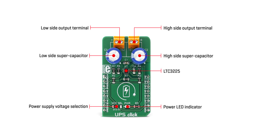
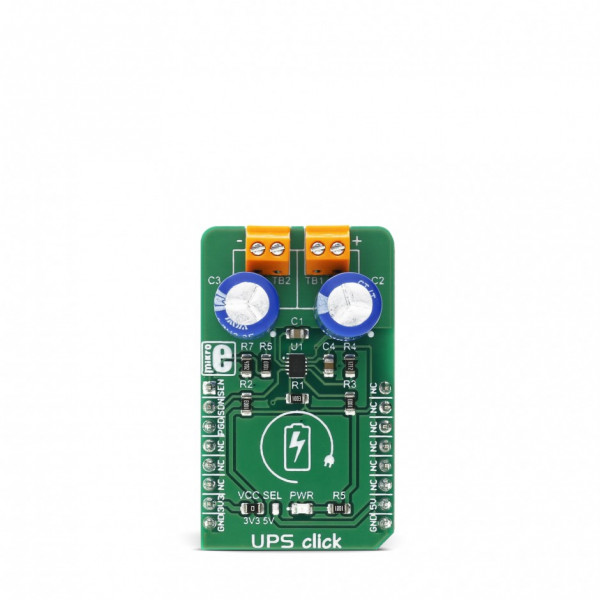
UPS click is a supercapacitor charger click that provides continuous power for a load connected to the output terminals. It also provides a temporary backup power supply in cases when the main power supply is abruptly disconnected - hence its name - UPS click. Besides backup function, it also provides a power for the applications with high peak power requirements, such as LED flashes, PCMCIA TX bursts, HDD bursts, GPRS/GSM transmitters and similar. UPS click uses two 3.3F supercapacitors connected in series, which are used as a temporary power storage banks.
This Click board™ has several key features, which allow efficient utilization of the supercapacitors: automatic cell balancing - for prevention of the capacitor overvoltage, low noise constant frequency charging - for a clean, noiseless power supply output, low power mode - when the input supply is removed the supercapacitors are not affected by the charging circuitry. It also requires a low count of external components and comes equipped with two connectors, which are used to connect the external load, but also to expand the capacity of the existing supercapacitors, if needed. These features allow UPS click to be used as a backup power source for a wide range of battery operated embedded applications.
How does it work?
The main active component of the UPS click is the LTC3225, a 150mA supercapacitor charger from Linear Technologies, used to charge two serially connected capacitors with a controlled current and constant voltage. The LTC3225 IC has the unique ability to maintain constant voltage level on both of the connected supercapacitors, by monitoring their voltages. This improves the lifecycle of the supercapacitors, protecting them from overvoltage. When a voltage difference occurs during charging (depending on the dissimilarities between the two used supercapacitors) the voltage across one of them might rise enough to cause a damage.

Unlike other balancing techniques that use resistors to discharge the capacitor which has a greater voltage, the LTC3225 automatically adjusts charging currents of two capacitors, until their charging speed is equal. Difference between the charging currents can be increased or decreased by 50%. When the Cout voltage reaches its nominal value (selected by the pull-up resistor on the Vsel pin to 5.3V), the internal charge pump is turned off, allowing the IC to enter the low power mode. The recharging cycle is automatically restarted when the voltage of the supercapacitors drops under a threshold.
The output terminals are used to connect an external load. There are two screw terminals routed to the output pins of each capacitor. Two supercapacitors are serially connected: the high-side capacitor has its positive pin connected to the Cout (a regulated voltage output pin), while the low-side capacitor has its negative pin connected to the GND. The negative pin of the high-side supercapacitor and the positive pin of the low-side supercapacitor are connected together and routed to the CX pin of the LTC3225, which is maintained at Cout/2. The voltage across a single terminal is, therefore, Cout/2, so to use the full range of the output voltage, a load should be connected between the high-side terminal labeled with the “+” sign, and the low-side terminal, labeled with the “-” sign. These terminals can also be used to connect additional supercapacitors, since the supercapacitors are in parallel with the connected load.
When the power source is turned off, the output voltage (Cout) depends only on used supercapacitors. These two supercapacitors have an equivalent capacitance of 1.65F and they will become the only elements that provide power for the connected load, when the power supply is removed. These capacitors will discharge through the connected load, and the output voltage will exponentially decrease according to the capacitor discharging formula.
The #SHDN pin can be used to put the device in the low power shutdown mode, by applying a LOW logic level. This pin is routed to the RST pin of the mikroBUS™ and it is labeled as SDN. It is pulled to a HIGH logic level by an on-board pull-up resistor.
It is possible to read the output voltage value by using the voltage divider, connected between the GND and the Cout. When the supercapacitors are fully charged, with the Cout voltage level of 5.3V, the value on the middle point of the voltage divider will be about 1.7V. The middle point of the voltage divider is routed to the AN pin of the mikroBUS™, allowing an easy analog to digital conversion by the host MCU. This pin is labeled as SEN on the Click board™.
The PGOOD pin of the LTC3225 IC is routed to the mikroBUS™ CS pin and it is labeled as PGD. This pin is an open-drain output and it is pulled to a HIGH logic level by an onboard resistor. When the output voltage reaches the value which is 6% below the nominal value, this pin is de-asserted. When the voltage drops under 7.2% below its nominal value, this pin is asserted and it is pulled to a LOW logic level. It can be used to monitor the state of the output supercapacitors.
The Click board™ uses power supply from the mikroBUS™. By moving the onboard SMD jumper labeled as JP1, it is possible to select either 3.3V or 5V rail as the input power source. It also selects the IC operating voltage, allowing interfacing with both the 5V and 3.3V MCUs. Regardless of the selected operating voltage, the output voltage is always 5.3V, as set by the Vsel pin of the UPS click.
UPS click uses only GPIO pins of the MCU for setting states on its pins, therefore it is extremely easy to work with. Nevertheless, there is a library provided for UPS click, which contains simple and clean functions for setting up its working parameters. These functions are demonstrated in the included application example, which can be used as a reference for a custom design.
Specifications
| Type | Battery charger |
| Applications | Can be used as a backup power source for a wide range of battery operated embedded applications, or when powering up current-limited applications with high peak power requirement |
| On-board modules | LTC3225 150mA supercapacitor charger from Linear Technology |
| Key Features | Automatic supercapacitor cell balancing, low noise constant frequency charging, low power mode with no influence on the supercapacitors charge, two high quality 3.3F supercapacitors onboard |
| Interface | GPIO |
| Input Voltage | 3.3V or 5V |
| Click board size | M (42.9 x 25.4 mm) |
Pinout diagram
This table shows how the pinout on UPS click corresponds to the pinout on the mikroBUS™ socket (the latter shown in the two middle columns).
Onboard settings and indicators
| Label | Name | Default | Description |
|---|---|---|---|
| LD1 | PWR | - | Power LED indicator |
| JP1 | VCC SEL | Left | Power Supply Voltage Selection 3V3/5V, left position 3.3V, right position 5V |
| TB1 | TB1 | - | Output connector parallel to the high side capacitor (C2) |
| TB2 | TB2 | - | Output connector parallel to the low side capacitor (C3) |
Software support
We provide a library for UPS click on our Libstock page, as well as a demo application (example), developed using MikroElektronika compilers. The demo application can run on all the main MikroElektronika development boards.
Library Description
This library presents some generic functions for controlling the Click board™.
Key functions:
void usp_setMode(uint8_t mode);- The functions for settings chip mode.uint8_t ups_getPowerGood();- The functions for reading the PGD state.
Examples Description
The demo application is composed of three sections:
- System Initialization - Initializes CS pin as INPUT and RST pin as OUTPUT.
- Application Initialization - Initializes Driver init and setting chip mode as ACTIVE.
- Application Task - (code snippet) - checks the state of PGD (Power Good), PGD goes high when Vout is within 6% of the target value (4.98V).
void applicationTask()
{
PGD_State = ups_getPowerGood();
if( PGD_State != 0)
{
mikrobus_logWrite("--- Power Good ", _LOG_LINE);
}
Delay_1sec();
}
The full application code, and ready to use projects can be found on our Libstock page.
mikroE Libraries used in the example:
- UART Library
- Conversions Library
- C_String Library
Additional notes and information
Depending on the development board you are using, you may need USB UART click, USB UART 2 click or RS232 click to connect to your PC, for development systems with no UART to USB interface available on the board. The terminal available in all MikroElektronika compilers, or any other terminal application of your choice, can be used to read the message.
mikroSDK
This click board is supported by mikroSDK - MikroElektronika Software Development Kit. To ensure proper operation of mikroSDK compliant click board demo applications, mikroSDK should be downloaded from the LibStock and installed for the compiler you are using.


