
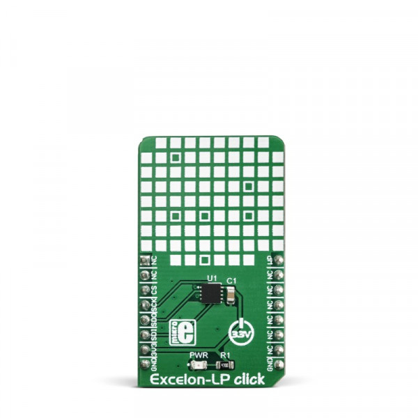
Excelon-LP click


Prices incl. GST
Out of Stock.
- Product Code: MIKROE-3104
- MPN: MIKROE-3104
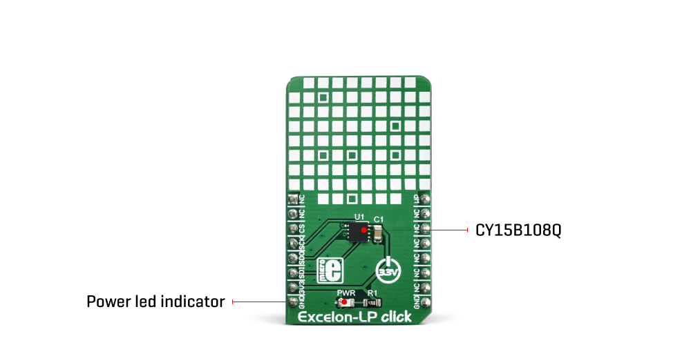
Excelon LP click uses the CY15B108Q, a serial FRAM module with 8 Mbit density. Although the FRAM is still being developed, this company managed to provide a very reliable and fast FRAM module that can write data at bus speed, has an extremely high endurance of 1014 read/write cycles, data retention period of 151 years, and very fast SPI interface.
Besides the unique technology used for the data storage, this device keeps the backward compatibility, in sense of communication and operation. Offering some outstanding features, as well as a range of standard features typically found on conventional EEPROM or FLASH modules, Excelon LP click is ideal for embedded applications which frequently execute write operations. It can be used for a wide range of applications, ranging from data collection, where the number of write cycles may be critical, to demanding industrial controls, where lengthy write intervals of conventional serial FLASH or EEPROM memory modules can cause data loss.
How does it work?
Excelon LP click is equipped with the CY15B108Q, a serial ferroelectric (FRAM) module with 8 Mbit density made by Cypress. It contains 1024 KB of available memory space. This memory module is manufactured using the ferroelectric technology, which has many advantages over the conventional technologies used for manufacturing conventional EEPROM and FLASH memory modules. Ferroelectric technology is still being developed and perfected, but the main advantages have already been demonstrated. This technology exploits the properties of ferroelectric materials to retain the electric field after they have been exposed to it, the same way the ferromagnetic materials retain the magnetic field. This phenomenon is employed to polarize the FRAM cells and store the information. One of the areas that still need to be improved is the thermal instability, especially on high temperatures. When the ferroelectric material reaches the Curie temperature, its properties are degraded. Therefore, exposure to high temperatures might damage the content of the FRAM module. This is illustrated by the data retention period, found in the datasheet: while working at 85?C, the data retention period is reduced to 10 years. At 65?C, the data retention period is over 150 years. Still, combined with the endurance of 1014 read/write cycles at bus write speed, this type of memory still represents an ideal solution for applications that must do a frequent writing to the non-volatile memory locations.
Excelon LP click uses the SPI communication protocol, allowing very fast serial clock rates. To ensure reliable data transaction and to avoid accidental write to the memory array, the device employs certain protection mechanisms. Before writing any data to the IC which modifies registers or the array itself, the WEL bit must be set. This bit is cleared after or during every memory modification instruction. Therefore, every memory modification instruction must be prefixed with the Write Enable (WREN) instruction that sets this bit to 1. This mechanism ensures that only the intended write instruction will be executed.
Communication with the device is initiated by the host MCU, which drives the chip select pin (#CS on the schematic) to a LOW logic level. This pin is routed to the mikroBUS™ CS pin. The next byte of information can be either command or data. Usually, the first byte is the instruction (command) followed by the memory address. Depending on the command that has been sent, either the memory is written to, or read from the specific memory address. Memory address on this device is 20-bit (0x000000 to 0x0FFFFF) and therefore it is sent by 3 bytes.
There are several instruction codes, which can be sent after the CS pin being driven to a LOW logic level. These include Write Enable, Write to the memory array, Read from the memory array, Write Status Register, Read Status Register, and so on. For a full list of commands and their detailed description, please refer to the datasheet of the CY15B108Q IC.
When using the Write to array instruction, it is possible to write the whole array, while keeping the CS line to a LOW logic level, as the internal address pointer will increase with each received byte of data. Once the end of the array is reached (address 0x0FFFFF) the internal pointer will rollover from the beginning (0x000000). An obvious advantage over the traditional EEPROM can be observed here: on a traditional EEPROM, the memory is organized in pages, usually 256 bytes long, which allow buffering of the data, because of the inherently slow write operation. The FRAM memory does not use pages, because the memory is written faster than the SPI bus can deliver new information (the data is written at bus speed). Therefore, no buffering is required, and the whole array can be sequentially written.
The CY15B108Q includes the option to write-protect specific parts or the whole memory array. The write protection mechanism consists of two bits in the Status Register (BP0, BP1). The Write Status Register instruction can be used to set or reset these bits. BP0 and BP1 bits control the write-protect status of the memory array (from one quarter to full memory array protection). These bits are non-volatile, and their state is retained between the power cycles.
The #WP pin is used to lock the Status Register. When this pin is driven to a LOW level, no further modifications to the Status register are possible and the instructions used to change bits in this register (Write Enable and Write Status Register) are completely ignored. Driving this pin to a LOW state effectively acts as the hardware memory write-protect lock mechanism. This pin can be completely disabled by the WPEN bit of the status register: if the WPEN bit is cleared (0), this pin will have no effect on the CY15B108Q IC. The #WP pin is routed to the mikroBUS™ PWM pin.
Specifications
| Type | FRAM |
| Applications | It can be used for a wide range of applications, from data collection, where the number of write cycles may be critical, to demanding industrial controls, where the long write time of serial FLASH or EEPROM modules can cause data loss |
| On-board modules | CY15B108Q, an 8 Mbit serial ferroelectric (FRAM) module from Cypress |
| Key Features | Built with the advanced FRAM technology, endurance of 1014 read/write cycles, data retention of over 150 years, industrial temperature range of –40?C to +85?C, high speed data transfer, low power consumption, no page buffering required |
| Interface | SPI |
| Input Voltage | 3.3V |
| Click board size | M (42.9 x 25.4 mm) |
Pinout diagram
This table shows how the pinout on Excelon-LP Click corresponds to the pinout on the mikroBUS™ socket (the latter shown in the two middle columns).
| Notes | Pin | Pin | Notes | ||||
|---|---|---|---|---|---|---|---|
| NC | 1 | AN | PWM | 16 | WP | Write Protect | |
| NC | 2 | RST | INT | 15 | NC | ||
| Chip Select | CS | 3 | CS | RX | 14 | NC | |
| SPI Clock | SCK | 4 | SCK | TX | 13 | NC | |
| SPI Data OUT | SDO | 5 | MISO | SCL | 12 | NC | |
| SPI Data IN | SDI | 6 | MOSI | SDA | 11 | NC | |
| Power supply | 3V3 | 7 | 3.3V | 5V | 10 | NC | |
| Ground | GND | 8 | GND | GND | 9 | GND | Ground |
Onboard settings and indicators
| Label | Name | Default | Description |
|---|---|---|---|
| LD1 | PWR | - | Power LED indicator |
Software support
We provide a library for the Heart rate 6 on our LibStock page , as well as a demo application (example), developed using MikroElektronika compilers. The demo can run on all the main MikroElektronika development boards.
Library Description
The library initializes and defines the SPI bus driver and drivers that offer a choice for writing data in memory and reading data from memory.
Key functions:
void excelonlp_sendCommand(uint8_t opcode)- Functions for send opcode commandvoid excelonlp_readData(uint8_t opcode, uint8_t *OUTBuf, uint8_t nData)- Functions for read datavoid excelonlp_writeMemoryData(uint8_t opcode, uint32_t addr, uint8_t _data)- Functions for write data to memoryuint8_t excelonlp_readMemoryData(uint8_t opcode, uint32_t addr)- Functions for read data form memory
Examples description
The application is composed of the three sections :
- System Initialization - Initializes SPI module and set CS and PWM pin as OUTPUT
- Application Initialization - Initializes Driver init
- Application Task - (code snippet) - Reads device ID, writes 6-bytes (MikroE) to memory and reads 6-bytes from memory
void applicationTask()
{
mikrobus_logWrite("Read Device ID : ", _LOG_TEXT);
excelonlp_sendCommand(_EXCELONLP_OPCODE_SET_WRITE_ENABLE_LATCH);
excelonlp_readData(_EXCELONLP_OPCODE_READ_DEVICE_ID, &OUTBuf[0], 9);
for(cnt = 0; cnt < 9; cnt++)
{
IntToHex(OUTBuf[cnt], demoText);
mikrobus_logWrite(" 0x", _LOG_TEXT);
mikrobus_logWrite(demoText, _LOG_TEXT);
Delay_100ms();
}
mikrobus_logWrite(" ", _LOG_LINE);
mikrobus_logWrite("Write MikroE data.", _LOG_LINE);
excelonlp_sendCommand(_EXCELONLP_OPCODE_SET_WRITE_ENABLE_LATCH);
for(cnt = 0; cnt < 6; cnt++)
{
excelonlp_sendCommand(_EXCELONLP_OPCODE_SET_WRITE_ENABLE_LATCH);
excelonlp_writeMemoryData(_EXCELONLP_OPCODE_WRITE_MEMORY_DATA, memoryAddress++, sendBuffer[cnt]);
Delay_100ms();
}
memoryAddress = 0x00000055;
mikrobus_logWrite("Read memory data : ", _LOG_TEXT);
for(cnt = 0; cnt < 6; cnt++)
{
MemoryData[0] = excelonlp_readMemoryData(_EXCELONLP_OPCODE_READ_MEMORY_DATA, memoryAddress++);
mikrobus_logWrite(MemoryData, _LOG_TEXT);
Delay_100ms();
}
Delay_ms( 5000 );
}
The full application code, and ready to use projects can be found on our LibStock page.
Other mikroE Libraries used in the example:
SPI
Additional notes and information
Depending on the development board you are using, you may need USB UART click, USB UART 2 click or RS232 click to connect to your PC, for development systems with no UART to USB interface available on the board. The terminal available in all MikroElektronika compilers, or any other terminal application of your choice, can be used to read the message.
mikroSDK
This click board is supported with mikroSDK - MikroElektronika Software Development Kit. To ensure proper operation of mikroSDK compliant click board demo applications, mikroSDK should be downloaded from the LibStock and installed for the compiler you are using.